


")
")
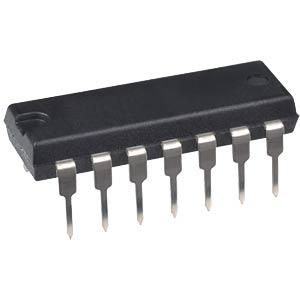
Introducing the CD4002BE IC DIP-14 Package (4002 IC), a versatile and essential integrated circuit designed to perform logical operations in electronic circuits.
This IC, also known as the 4002 IC, is a fundamental building block for various digital applications.
The 14-pin dual in-line package simplifies the connection process, so making it suitable for prototyping, experimentation, and inclusion in various electronic projects.
This makes it an efficient choice for battery-powered devices and applications where signal integrity is crucial.
In terms of functionality, the CD4002BE IC is a dual 4-input NOR gate, providing logical operations based on multiple inputs.
Each of its two NOR gates accepts four binary inputs and produces a single output, making it valuable in circuit designs that require logical combinations of signals.
Furthermore, the CD4002BE IC is known for its robust design and reliable performance across a range of operating conditions.
Its versatility extends to various digital applications, including arithmetic circuits, memory units, and more complex logic circuits.
Features :-
- Standardized symmetrical output characteristics
- 100% tested for maximum quiescent current at 20 V
- 5-V, 10-V, and 15-V parametric ratings
- Propagation delay time = 60 ns (typ.) at CL = 50 pF, VDD = 10 V
- Buffered inputs and outputs
- Maximum input current of 1 µA at 18 V over full package-temperature range; 100 nA at 18 V and 25°C C
- Noise margin (over full package temperature range): 1 V at VDD = 5 V 2 V at VDD = 10 V 2.5 V at VDD = 15 V
- Meets all requirements of JEDEC Tentative Standard No. 13B, “Standard Specifications for Description of ’B’ Series CMOS Devices
To Learn More Visit our Website
For more information:-www.mifraelectronics.com
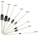
* Product Images are shown for illustrative purposes only and may differ from actual product.
Package Includes:
- 1 x CD4002BE IC DIP-14 Package (4002 IC).

Reviews
There are no reviews yet.